High-Speed PCB Design
Via Stitching / Fencing
Uniform Ground Potential
Ground plane has resistance
Vias (or ground pins) etc. helps to keep ground potential as uniform as possible under current flow.
Thermal Dissipation
Vias are much better heat dissipators than FR4.
Return Path
Return currents follow path of least impedance.
At low frequencies / DC, return current is shortest path between trace start and end in ground plane (least resistance). At high frequencies, return current follows trace in reference plane (least inductance by minimizing loop area). 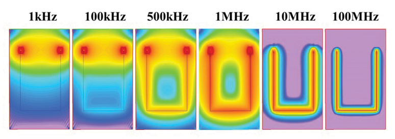
Higher Current Flow
Stitch multiple track layers to increase current capacity
Perimeter Via Fencing
Faraday Cage (λ/10 spacing)
Reduces received and emitted EM radiation. Do this together with the 3H copper pour pullback guideline.
Crossing Layers
Ground via when changing reference plane
Or else the return current will spread out in a nasty matter across the original reference plane to find the nearest via.
References
- https://electronics.stackexchange.com/questions/371559/why-try-to-maximize-number-of-grounding-vias-in-rf-pcbs
- https://www.emcs.org/acstrial/newsletters/fall08/tips.pdf
- https://rushpcbinc.com/what-is-via-stitching-and-why-it-is-useful/
- https://www.ndsu.edu/pubweb/~braaten/EMC_2016_1.pdf
- https://incompliancemag.com/article/alternative-paths-of-the-return-current/
- https://www.youtube.com/watch?v=nPx2iqmVAHY
- https://www.youtube.com/watch?v=S6PNYKxJsdk
- https://circuitdigest.com/article/here-is-why-you-should-use-via-stitching-for-your-next-pcb-design
Routing Directions
Goal: reduce cross talk
Configure your board layers so that two adjacent signal layers will have preferred routing directions that cross each other instead of running parallel to each other. If layer two is running “north to south,” then make sure that layer three is running “east to west.” In this way you can minimize the possibility of broadside coupling.
Other
- Avoid return path discontinuity (i.e. ensure full ground polygon adjacent to high speed traces)
- Impedance Matching (simple transmisson line stuff, reduce loss)
- Termination (reduce reflection)
Concepts
- Every circuit is a loop (hence inductance), capacitance comes from dielectric
- Conductors carry current, non-conductors carry EM waves
- Multiple decoupling capacitors are needed because of inductance (so they block different frequencies as that are not just a simple RC)
To-Read
- https://www.protoexpress.com/blog/effects-high-speed-signals-pcb-design/
- https://www.microwavejournal.com/blogs/1-rog-blog/post/24374-comparing-microstrip-and-grounded-coplanar-waveguide
- https://www.electronics-notes.com/articles/basic_concepts/inductance/inductance-of-straight-wire-coils.php